Environmentally Conscious and Economically Sound Machine Dismantling Forum > Kenosha
> Tips and Advices
> 300MM polished silicon wafer 12" 12 inch 300 mm si
300MM polished silicon wafer 12" 12 inch 300 mm si
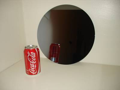
300 mm Silicon Wafer, polished to an incredible mirror finish on both sides.
These are the starting point for integrated circuits. The 300 mm wafers are the largest currently available, and are sometimes described as 12" wafers (although the true dimension is slightly smaller than 12 inches.)
Why would anyone want one of these? They are an amazing product of state-of-the-art technology. The purity of the silicon exceeds almost anything else you will ever encounter, either man-made or natural. It is the largest object made from a single, perfect crystal that most people will ever see. They are cut and polished to a flatness that is truly remarkable, using incredibly expensive precision equipment.
The visual impact of a 300 mm wafer is hard to describe. It has over twice the area of an 8" wafer, once the "monster" of the semiconductor world.
Once you've seen one in person, you either think they are incredibly cool, or you don't. It's a nerd thing.