Environmentally Conscious and Economically Sound Machine Dismantling Forum > Madison, WI
> Electrical Machinery
> Transformers
> Olympus bhmjl semi-conductor microscope, complete
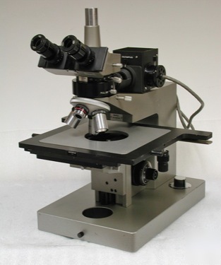
Olympus bhmjl semi-conductor microscope, complete
This listing is for a very nice Olympus semi-conductor inspection microscope, model BHM-JL. It includes a massive stage with a scanning area of better than 150 x 150 mm.
This particular instrument includes the in-base step transformer capable of running either a 12v 50w halogen lamp, or a conventional 6v20w tungsten lamp (switch selection on back panel with separate jack for each lamp type). The microscope frame is of massive proportions and very deflection-free. The stage focus drive runs on a very large bearing that is completely free of play - stage does not wobble in the slightest even with the 40x objective. The course / fine focus block is very responsive and also very free of backlash.
The specimen stage is also very free of backlash, and operation is smooth in both X and Y axis throughout the range. Notably, this stage also includes the steel racks in both directions (some stages used plastic molded racks, many of which have shrunk over time causing the teeth to fail). The stage can be interchanged - it is mounted with a large dovetail bearing and clamp (visible beneath the stage in the second photo).
NEO PLAN 10 (0.25 na, achromat flat field)
NEO PLAN 20 (0.40 na, achromat flat field)
NEO PLAN 40 (0.65 na, achromat flat field)
All four objectives are of the shorter 37 mm adjustment length, and as mentioned in the discussion of the vertical illuminator, are not infinity corrected.
A couple of words on the condition of the instrument. The stand does have a couple of minor scratches where a label was removed on the side of the stand, and a bit of wear on some corners. The two little foils that cover the fine adjustment knobs are missing. The stage does have some very minor scuffing on a couple of the upper corners, and the chrome tube for the camera port does show some evidence of items having been clamped there. These are all exceedingly trivial cosmetic issues. Functionally, the microscope is in superb condition throughout, and the lenses are all spectacular. This instrument was certainly never abused - on the contrary, it appears to have been very well cared for.
To illustrate the darkfield capability of the microscope, instead of shooting some photos of semiconductor wafers I decided to do something a bit more unusual. The photos were taken with the Neo Plan 10 and the Neo Plan 20 objectives, and were of a polished thick section of rock taken from a deep-sea drill core sample. It is a bit more interesting than most wafers. . . I only wish the photos could convey the quality of these lenses - the images in the oculars are quite stunning.
Thank you for looking at this listing. I welcome any questions you may have and will do my best to answer them!